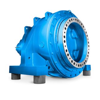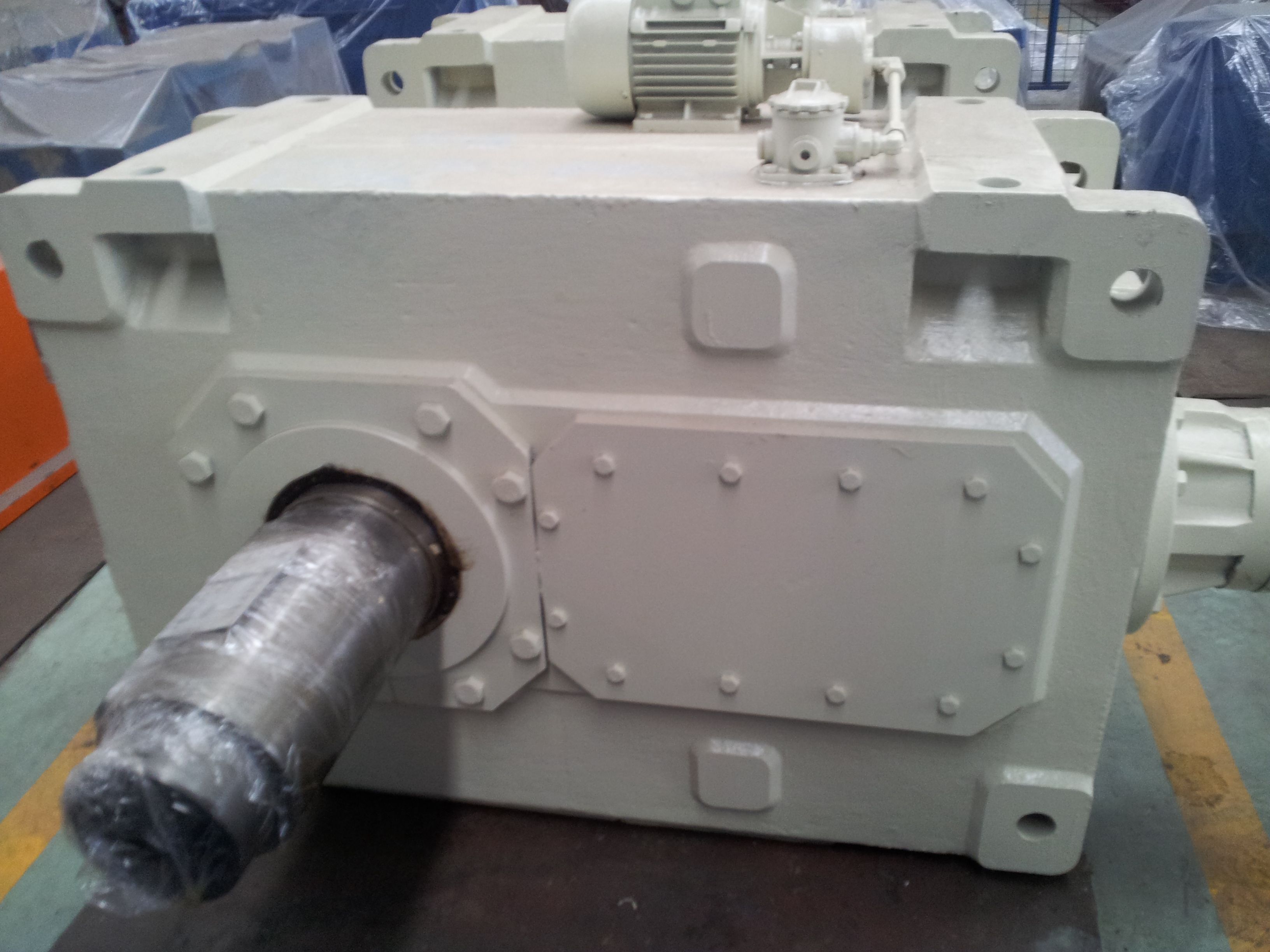
Bevel-helical speed reduction gearboxes B4 ystem simultaneously the same effect can be achi B4FH-18-C
In stock
SKU
B4FH-18-C
$111,428.57
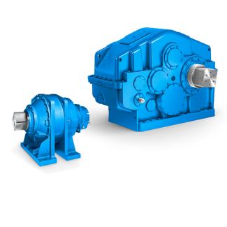
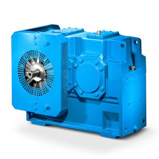
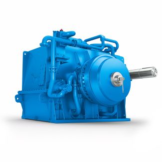
Flender/Flender Gear Units/Bevel-helical speed reduction gearboxes B4
with layer thickness of 2 to 4 [MCrIm. If required, the Cu surface can be protected with coatings. pilot installation which produces hi quality, reproducible Cu foils of low ductility in con-' tinuous process was developed for tk-manufacture of this
  hot-stamping foil. The experience gained with this pilot installation formed the basis for the conceptual prepara- tion of an industrial-scale
  plant. 3.2. Development of hot-stamping method for flat and curved surfaces In the hot-stamping process, the adhesive layer is activated
  by pressure and heat on the raised areas of the stamping block(identica1 to the PCB configuration), and the printed conductor pat- tern is transferred to the substrate to be stam ed Under the effects of heat, the parting layer located between the copper layer and the bac6ngsheet dissolves the foil bond on theareas to . be stamped. few seconds after the stamping time (0.5 - 3 sec.) has elapsed, the composite sheet can be removed from the stamped substrate. The adhesive layer can be subjected to loading after approx. 1 . sec. After the stamping rocess, the bond between the backing sheet and the residual copper film remains intact on alpsurfaces which were not heated by the raised areas of the stamping block. while the printed conductors adhere to the substrate. When the composite sheet is subsequently removed from the substrate, the residual copper adheres to the backing sheet and is pulled off with it. The backing sheet has ne ative effect on the stampable conductor widths and acings Therefore, techniquewasdleveloped bywhichtheCufoilcan be processedwithouttRe back: ing sheet. In this context, the Cu foil is stamped and the excess copper, which otherwise ad- heres to the backing sheet, is removed by rolling adhesive tape over the stamped circuit. semi-automatic stamping machine with turntable was developed for this process. The processing steps are: hot-stamping, rolling over with adhesive tape to remove excess cop-
| Model Type | Bevel-helical speed reduction gearboxes B4 |
|---|---|
| Gear Type | Bevel Helical Gear |
| Weight (kg) | 5200.000000 |
| Ratio Range | 1 : 90…355 |
| Low Speed Output | Flanged shaft |
| Nominal Torque | 240000 Nm |
| Mounting Arrangements | Horizontal mounting position |
| Manufacturer | A. Fried. Flender AG |
| Country of Manufacture | Papua New Guinea |
| Data Sheet & Drawings | Bevel-helical speed reduction gearboxes B4 ystem simultaneously the same effect can be achi B4FH-18-C |
Related Products